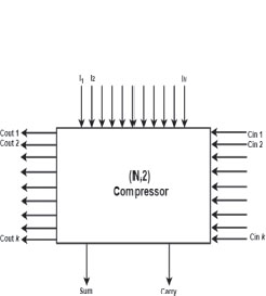
Figure 1. Compressor Circuit
Energy Efficient Compressor Cell for Low Power Computing
Rahul Mani Upadhyaya, R. K. Chauhana and Manish Kumara
a Madan Mohan Malaviya University of Technology, Gorakhpur, Uttar Pradesh, India
ABSTRACT
As the use of multimedia devices is rising, power management is becoming a major challenge. Various types of compressors have been designed in this study. Compressor circuits are designed using several circuits of XOR-XNOR gates and multiplexers. XOR-XNOR gate combinations and multiplexer circuits have been used to construct the suggested compressor design. The performance of the proposed compressor circuits using these low-power XOR-XNOR gates and multiplexer blocks has been found to be economical in terms of space and power. This study proposes low-power and high-speed 3-2, 4-2, and 5-2 compressors for digital signal processing applications. A new compressor has also been proposed that is faster and uses less energy than the traditional compressor. The full adder circuit, constructed using various combinations of XOR-XNOR gates, has been used to develop the proposed compressor. The proposed 3-2 compressor shows average power dissipation 571.7 nW and average delay 2.41 nS, 4-2 compressor shows average power dissipation 1235 nW and average delay 2.7 nS while 5-2 compressor shows average power dissipation 2973.50 nW and average delay 3.75 nS.
KEYWORDS
full adder; delay; power dissipation; power-delay product; XOR-XNOR gates
1. Introduction
Modern technological devices are now becoming smaller, quicker, as well as less costly. This has been accomplished through very-large-scale integration (VLSI) technology scaling which has enabled rapid growth in device density and operational rate (Tonfat et al., 2012). The demand for low power electronics and communication systems is driven by technology scaling and marketing. Low power is required in devices such as laptops, digital watches, pacemakers and cellular phones. High performance is achieved by increasing the number of transistors in silicon chip, which increases the packaging density of the chip but simultaneously increases power dissipation, leading to packaging and reliability problems. The lack of reliability is caused by the increasing temperature which affects the performance of the circuit (Chang et al., 2004).
Low power as well as design reliability must always be considered at all levels of development. The selection of logical patterns is vital for every design at the module level because it greatly influences power and reliability. Static complementary metal-oxide semiconductors (CMOS) and domino circuitry are inadequate for forthcoming computing needs. Static logic and dynamic logic are two fundamental CMOS circuit architectures (Esposito et al., 2018). Static CMOS seem to be more energy-efficient and resilient, but it is extremely sluggish when employed in important or large-scale circuits. With an overwhelming use of battery-operated digital device in the past few decades, it is demand of the VLSI industry to design energy-efficient digital circuits. Since arithmetic logic units (ALU) are at the heart of digital circuits, arithmetical operation needs to be performed faster and with less power consumption (Venkatachalam et al.,2017).
The addition of partial product terms by compressor is the most frequent operation done in ALU by digital circuits (Esposito et al., 2018). Sometimes, other operations are associated with the yields of the compressor and the delay in the outputs leads to delay in the overall performance of the device. The battery technology is advancing at a slower rate as compared to the microelectronics industry (Esposito et al., 2018). So, the availability of power is limited for battery operated digital circuits and to ensure devices have long operating time, low power compressor design has become an important design consideration.
According to Moore’s law], the increase in the transistor on a chip doubles every 24 months (Zakian et al., 2020). Increment in the transistor on same chip area results is more power dissipation which consequently results in the devices’ poor performance. Therefore, the transistors count of digital devices needs to be reduced by arranging the transistors in proper logical manner. In a nutshell, it can be said that enhancing the performance of the compressor is becoming an important goal of modern microprocessor industry and therefore VLSI researchers are developing energy efficient techniques for reducing power dissipation and delay in compressors to ensure longer life, better reliability, and fasteroperation (Ha et al., 2018).
1.1. Sources of Power Dissipation
There are three sources of total power dissipation in digital CMOS circuits, they comprise the summation of two components: dynamic or switching power dissipation and static power dissipation.
1.1.1. Dynamic Power Dissipation
Dynamic power is one that is dissipated by charging and discharging the internal load capacitances. Let us consider load capacitance CL is switched between the ground and supply voltage at the switching frequency f. At any given time interval of T, the charging and discharging time interval of load capacitance is Tf times. During the charging phase, load capacitance CL of the output node is charged from 0 to VDD it makes full transition (Yang et al., 2015). The pMOS is conducting during the charging phase of load capacitance CL and half of the energy is wasted in the form of heat and it drags from the power supply. During the discharging phase, half of the energy which is already accumulated in load capacitance (CL) is discharged and the output node voltage drops from VDD to 0. When nMOS is conducting, no energy is wasted in the form of heat. A total charge in load capacitance Q = CV is transferred from VDD to ground in one complete cycle of charging/discharging the capacitance (Nirlakalla et al., 2011).
Dynamic average power dissipation is:
In that time total charge is delivered:
The switching frequency can be expressed as activity factor α time of the clock frequency because gates do not switch at every clock cycle:
Every clock cycle has activity factor α =1 in each rise and fall cycle. In each cycle, the maximum activity factor is 0.5.
The switching power expression can be derived by considering the charge up and charge down phase at output node of CL (load capacitance). In CMOS logic gates, internal circuit has full or partial transition of voltage during switching. The overall power dissipation in a CMOS circuit is due to the transition of the internal voltage, however, these voltage transition is considered when output voltage is changed, indeed internal node voltage changes many times.
1.1.2. Short-Circuit Power Dissipation
Short-circuit power is dissipated by instantaneous short circuit connection between the VDD and GND at the time when the gate switches. From the above discussion we infer that the switching power is independent to the rise time and fall time of the input voltage and that it is required in the circuit to charge up the internal parasitic load capacitance. In this research authors take an example of CMOS inverter which is operated with finite rise time and fall time of the input signal; both pMOS and nMOS transistors are turned on simultaneously. At the same time, for a short period of time, there is a direct current flow from VDD and 0 during switching. A short circuit current flows from both (nMOS & pMOS) transistors at switching time but it does not provide any charging to internal load capacitance in circuit, hence, it is known as a short circuit current. The nMOS transistor starts conducting when input voltage exceeds the threshold, the voltage Vtn of nMOS transistor and pMOS transistor remains turned on until the level of input voltage reaches (VDD -|Vtp|). Let us assume that CMOS inverter is identical where the rise time and fall time of input is the same, the magnitude of the short circuit current depends on the rising and falling input transition. The small load capacitance (CL) charge of the pMOS transistor falls, however only during input transition, and nMOS transistor conducts only when input transition is rising. The switching power dissipation in a circuit is responsible for this current component, total power dissipation drawn from power supply is determined by calculating the mean of these current components.
Let us assume that a symmetrical CMOS inverter has transconductance kn =kp = k, threshold voltage Vtp=Vtn=Vth with small load capacitance and rise time and fall time equal (Ʈn=Ʈp=Ʈ); average short circuit current is derived:
Short-circuit power dissipation is expressed as:
The short-circuit power dissipation is proportional to the rise and fall time of the input voltage and it also depends on the transconductance of the circuit. Hence, short circuit current can be minimized by reducing the transition time of the input voltage.
1.1.3. Static Power Dissipation
In CMOS, logic gates are used in pMOS and nMOS transistors, which generally have a small amount of (reverse and subthreshold) leakage current. The magnitude of the two current components, reverse and subthreshold, is considered for the total dissipation of power when the circuit is undergoing non conducting mode because millions of transistors are fabricated in a single silicon chip (Leon et al., 2018). The leakage current magnitude is mainly calculated by processing parameters. The static power dissipation directly depends on static current and supply voltage (Esposito et al., 2018).
2. Conventional Compressor Design
A compressor is a combinational circuit that takes N inputs bits and generates a Sum and Carry bits as shown in Fig 1. Although compressor gives same outputs as full adder but it is different from a conventional adder. For example, compressor adds N-bits of the same precision whereas an adder adds two operands of N-bit numbers of deferring precision (Kumar et al., 2014). A (M, N) parallel counter N-bits count of the number of M-bits that have logic ones. But counter differ from compressor as compressor has “Carry-inputs” and “Carry-outputs” in addition with the inputs whereas these features are absent in the counters.
Figure 1. Compressor Circuit
With the growing popularity of multimedia gadgets, power management has become a major issue. The primary energy-consuming components in these gadgets are multipliers. The 3-2, 4-2, and 5-2 compressors are the fundamental elements in numerous applications, such as partial product summation in multipliers. Compressors are four/five/six/seven bit adder circuits with three outputs. Compressors are required for high speed multipliers (Qian et al., 2016). The efficiency of the compressors is directly related to the multipliers' speed, size, and power consumption. In this section we are going to discuss various high-performance compressors, designed by researchers working in this area.
(Reddy et al., 2019) has proposed a novel design of approximate 4-2 compressor. By conducting experimental analysis, the authors have found that the proposed design has signification reduction in the error as compared to similar compressors found in open literature. The efficiency of the proposed compressor and multiplier was evaluated in a 45 nm standard CMOS technology through extensive experimental evaluation, and their parameters were compared with the approximate multipliers. When compared to other approximate compressors available in the literature, the proposed compressor achieved a significant reduction in error rate. Furthermore, the proposed multiplier reduces power consumption, delay, and area by 35%, 36%, and 17%, respectively, when compared to the exact multiplier. Some image processing applications evaluate the multiplier's effectiveness. The proposed multiplier processes images with 85% structural similarity to the exact output image on average. When compared to the exact multiplier, the proposed multiplier shows a significant improvement in terms of power consumption and delay.
Further, to reduce the power consumption and enhance the energy efficiency of the approximate 4-2 compressor, (Pei et al., 2020) have reduced the number of output numbers to one. The method lowered the amount of approximate 4-2 compressor outputs to one, which improved energy efficiency even further. The simulation results showed that the proposed approximate compressors UCAC1, UCAC2, and UCAC3 achieved a 24.76%, 51.43%, and 66.67% reduction in delay, 71.76%, 83.06%, and 93.28% reduction in power, and 54.02%, 79.32%, and 93.10% reduction in area, respectively, when compared to the exact 4-2 compressors. The use of the proposed compressors in 8-bit multipliers resulted in a mean power consumption reduction of 49.29%.
(Ansari et al., 2018) reduced the number of faulty rows in the compressor's truth table by encoding its inputs using generate and propagate signals. The proposed multipliers were tested using image sharpening and JPEG applications. M16-5, which produces more accurate output than other approximate multipliers, achieved higher quality. In image sharpening and Joint Photographic Experts Group (JPEG) applications, the proposed multipliers outperformed other approximate designs by achieving higher quality outputs with lower power consumption.
(Ha et al., 2018) proposed an approximate 4-2 compressor design that includes an error recovery module. With this suggested architecture, an approximate 8-32 bit multiplier utilizes 23.2-24.4% less hardware space, 22.4-25.0% less energy, and 11.2-17.0% less latency compared to an exact multiplier. It is noteworthy that none of the choices were necessary to improve all three measures simultaneously. The proposed multiplier design, as per error analysis, reduces the mean error distance (MED) of multiplication results by at least 11.7% compared to earlier approximation multiplier designs.
2.1. 3:2 Compressor
The compressor is used extensively in combinational circuits to add partial product terms by cascading full adder. The primary circuit for designing a 3:2 compressor is full adder which is further integrated together to obtain higher order compressor such as 4:2, 5:2 etc. 3:2 compressor takes in three inputs, namely X1, X2 and X3, and produces two outputs which are sum bit S and the carry bit C which is shown in Fig. 2(a). The 3:2 compressor is governed by the equation:

Figure 2 (a). Conventional architecture of 3:2 compressor
The 3:2 compressor can be designed as the circuit of full adder by considering third input as Cin ‘carry- in’ from the previous block. It is clearly visualized from conventional implementation of 3:2 compressor that XOR and MUX are the two important building blocks of the compressor shown in Fig. 2(b), which determines the performance of the compressor (Yi et al., 2019).

Figure 2 (b). 3:2 compressor using XOR module and MUX circuit
MUX gates and an XOR–XNOR gate makes up the proposed compressor circuit. Low power dissipation, fast speed and full-swing output are all advantages of this versatile structure. XOR/XNOR gate minimizes the power consumption of the proposed compressor circuit and a NOT gate creates the other XOR or XNOR signal shown in Fig 3. The NOT gate is used to boost the circuit's output driving capabilities (Momeni et al., 2015). The capacitance of input A and input B of the XOR circuits is not symmetric as one input should be attached to the NOT gates' input and the other input should be linked to the nMOS transistor diffusion. Furthermore, in the ideal condition the capacitance of input A and input B is not equal for minimum PDP shown in Fig 5. Schematic diagram of the proposed 3:2 compressor is shown in Fig 4. In addition, the function of circuit operation is not affected by the order in which the connections between the inputs and the transistors are made (Lee et al., 1997).

Figure 3. Proposed 3:2 compressor circuit

Figure 4. Schematic diagram of the proposed 3:2 compressor

Figure 5. Input and output waveforms at 1 volt
2.2. 4:2 Compressor
Further, this hybrid full adder is utilized to design 4:2 compressor. The proposed 4:2 compressor finds a wide range of applications in multipliers, microprocessor (Wang et al., 2006). A 4:2 compressor has four inputs (X1, X2, X3, and X4) and two outputs (Sum and Carry). It also has a carry-in input from previous lower significant compressor [Akbari et al., 2017]. The output Cout is output to the next significant stage. A 4:2 compressor block is portrayed in Fig. 6 (a). 4:2 compressor using full adder circuit is shown in Fig. 6 (b). The equation governing a 4:2 compressor is provided below:

Figure 6 (a). Conventional architecture of 4:2 compressor
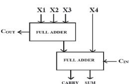
Figure 6 (b). 4:2 compressor using full adder circuit
As illustrated in Fig. 7, 4-2 compressor is traditionally implemented with two serially connected full adders. XOR gates are anatomized from high input compressors at the gate level, and carry generators that are traditionally implemented by multiplexers (MUX). Input and output waveform at 1 volt of 4-2 compressor is shown in Fig. 8.

Figure 7. Simulated circuit of proposed 4:2 compressor

Figure 8. Input and output waveforms at 1 volt
2.3. 5:2 Compressor
The 5-2 compressor is another typical component for high-precision and high-speed multipliers (Kumar et al., 2014). The block diagram of a 5-2 compressor with seven inputs and four outputs is shown in Fig. 9 (a). X1, X2, X3, X4, and X5 are the principal inputs, whereas Cin 1 and Cin 2 are the secondary inputs (Xu et al., 2016). All seven inputs have the same weights. 5:2 compressor using full adder circuit is shown in Fig. 9 (b). The 5-2 compressor generates a sum output with the same weight as the inputs. The outputs of Cout 1 and Cout 2 are routed to a larger neighboring compressor. Input and output waveform at 1 volt of 5-2 compressor is shown in Fig. 10.

Figure 9 (a). Conventional architecture of 5:2 compressor
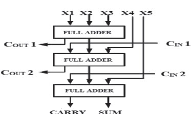
Figure 9 (b). 5:2 compressor using full adder circuit

Figure 10. Input and output waveforms at 1 volt
3. Performance Metric of Proposed Compressor
The schematic diagrams of the proposed 3:2 compressor, 4:2 compressor and 5:2 compressor portrayed in Figures 3 - 10 where full adders are employed in the design. Three inputs are given to the first full adder which adds them and produces the output. The sum output is fed to the second full adder along with fourth input and Cin. The second full adder adds them and finally produces sum and carry outputs. The proposed 3:2 compressor, 4:2 compressor and 5:2 compressor are simulated using Cadence EDA tool for the voltage range of 0.5 V to 2 V and outputs of 3:2 compressor is shown in Table 1, outputs of 4:2 compressor is shown in Table 2 and outputs of 5:2 compressor is shown in Table 3.
Table 1. Performance parameters comparison of 3:2 compressors (0.5 V to 2.0 V)
Vdd (V) |
0.5 |
1.0 |
1.5 |
2.0 |
References |
Power Dissipation (nW) |
|||||
LPHS |
56.58 |
225.09 |
556.40 |
2122 |
[Ha et al.] |
NOVEL CA |
49.85 |
216.86 |
490.26 |
1850 |
[Yi et al.] |
Proposed Work |
42.30 |
143.20 |
448.30 |
1653 |
|
Delay (nS) |
|||||
LPHS |
8.03 |
2.36 |
1.22 |
0.67 |
[Ha et al.] |
NOVEL CA |
7.11 |
2.20 |
0.96 |
0.56 |
[Yi et al.] |
Proposed Work |
6.28 |
2.07 |
0.83 |
0.49 |
|
Power Delay Product (x 10-18J) |
|||||
LPHS |
454.33 |
531.21 |
678.80 |
1415 |
[Ha et al.] |
NOVEL CA |
353.43 |
477.09 |
470.64 |
1036 |
[Yi et al.] |
Proposed Work |
265.644 |
296.42 |
372.08 |
809.97 |
|
Table 2. Performance parameters comparison of 4:2 compressors (0.5 V to 2.0 V)
Vdd (V) |
0.5 |
1.0 |
1.5 |
2.0 |
References |
Power Dissipation (nW) |
|||||
LPHS |
343.60 |
1114.10 |
3228.39 |
4545.92 |
[Ha et al.] |
NOVEL CA |
211.85 |
943.86 |
2347.26 |
2992.91 |
[Yi et al.] |
Proposed Work |
112.3 |
706.70 |
1841 |
2280 |
|
Delay (nS) |
|||||
LPHS |
10.35 |
1.78 |
0.80 |
0.57 |
[Ha et al.] |
NOVEL CA |
8.92 |
1.54 |
0.81 |
0.59 |
[Yi et al.] |
Proposed Work |
8.11 |
1.42 |
0.69 |
0.58 |
|
Power Delay Product (x 10-18J) |
|||||
LPHS |
3556.26 |
1983.08 |
2582.71 |
2591.17 |
[Ha et al.] |
NOVEL CA |
1889.70 |
1453.54 |
1901.28 |
1765.81 |
[Yi et al.] |
Proposed Work |
910.75 |
1003.51 |
1270.29 |
1322.40 |
|
Table 3. Performance parameters comparison of 5:2 compressors (0.5 V to 2.0 V)
Vdd (V) |
0.5 |
1.0 |
1.5 |
2.0 |
References |
Power Dissipation (nW) |
|||||
LPHS |
323.16 |
2464.11 |
6448.34 |
9890.12 |
[Ha et al.] |
NOVEL CA |
211.71 |
1883.25 |
5647.54 |
8678.34 |
[Yi et al.] |
Proposed Work |
136.0 |
1110 |
3358 |
7290 |
|
Delay (nS) |
|||||
LPHS |
12.33 |
2.01 |
0.91 |
0.62 |
[Ha et al.] |
NOVEL CA |
12.15 |
2.11 |
1.00 |
0.69 |
[Yi et al.] |
Proposed Work |
11.57 |
1.90 |
0.91 |
0.65 |
|
Power Delay Product (x 10-18J) |
|||||
LPHS |
3984.56 |
4952.86 |
5867.98 |
6131.87 |
[Ha et al.] |
NOVEL CA |
2572.27 |
3973.65 |
5647.54 |
5988.05 |
[Yi et al.] |
Proposed Work |
1573.52 |
2109 |
3055.78 |
4738.50 |
|
The performance parameter for the proposed compressor i.e., power dissipation came to be nW and delay in nS. It can be observed from Table 1, Table 2 and Table 3 that the proposed full adder has better performance.
3.1. Temperature Analysis
The data analysis proved the aforesaid effect of temperature on digital circuits. It increases almost linearly with increase in temperature at lower voltages (-30 ºC to 70 ºC) and increases exponentially with further increase in temperature as can be easily seen in Table 4. The power dissipation increases at higher temperature ranges due to the increase in leakage current. Hence, the proposed circuit has almost stable output at lower temperature ranges which define the robustness of the proposed design. The measured power dissipation at different temperatures is tabulated in Table 4.
Table 4. Effect of temperature on dissipated power (x10-6 W) on proposedcircuits
Temperature (0C) |
3:2 Compressor |
4:2 Compressor |
5:2 Compressor |
-30 |
0.198 |
0.683 |
1.087 |
-20 |
0.200 |
0.687 |
1.094 |
-10 |
0.203 |
0.691 |
1.100 |
00 |
0.205 |
0.696 |
1.107 |
10 |
0.207 |
0.700 |
1.110 |
20 |
0.209 |
0.704 |
1.111 |
30 |
0.211 |
0.708 |
1.113 |
40 |
0.213 |
0.711 |
1.116 |
50 |
0.215 |
0.714 |
1.117 |
60 |
0.216 |
0.718 |
1.111 |
70 |
0.218 |
0.721 |
1.120 |
4. Conclusion
This research has proposed a new high-speed, low-power energy-efficient compressor circuit. The full adder design has been utilized to design a higher order compressor i.e., 3:2, 4:2 and 5:2 compressor as presented in figure. This compressor is an important part of multiplier. The compressor has been further simulated with the Cadence EDA tool using 45 nm CMOS process technology. The performance parameters were recorded and tabulated. This compressor had less delay and low power dissipation. The transistor count also reduced. Therefore the proposed compressor can be used in numerous applications such as multiplier, DSP microprocessor and data processing systems. For a supply ranging from 0.5 V to 2V, the suggested compressor's speed, power, and PDP were computed. The proposed design achieved considerable improvements in terms of power consumption and speed. This novel compressor's performance was also compared to that of a variety of currently available compressors described in the literature. According to simulation results, the proposed 4-2 compressor shows average power dissipation 1235 nW and average delay 2.7 nS while 5-2 compressor shows average power dissipation 2973.50 nW and average delay 3.75 nS.
5. References
Akbari, O., Kamal, M., Afzali-Kusha, A., & Pedram, M. 2017. Dual-Quality 4:2 Compressors for Utilizing in Dynamic Accuracy Configurable Multipliers. IEEE Trans. Very Large Scale Integr. (VLSI) Syst., 25(4), 1352–1361. https://doi.org/10.1109/TVLSI.2016.2643003
Ansari, M. S., Jiang, H., Cockburn, B. F., & Han, J. 2018. Low-power approximate multipliers using encoded partial products and approximate compressors. IEEE Journal on Emerging and Selected Topics in Circuits and Systems, 8(3), 404–416. https://doi.org/10.1109/JETCAS.2018.2832204
Chang, C. H., Gu, J., & Zhang, M. 2004. Ultra low-voltage low-power CMOS 4-2 and 5-2 compressors for fast arithmetic circuits. IEEE Trans. Circuits and Syst., 51(10), 1985–1997. https://doi.org/10.1109/TCSI.2004.835683
Esposito, D., Strollo, A. G. M., Napoli, E., & Petra, N. 2018. Approximate Multipliers Based on New Approximate Compressors. IEEE Trans. Circuits and Syst., 65(12), 4169–4182. https://doi.org/10.1109/TCSI.2018.2839266
Ha, M., & Lee, S. 2018. Multipliers with Approximate 4-2 Compressors and Error Recovery Modules. IEEE Embedded Systems Letters, 10(1), 6–9. https://doi.org/10.1109/LES.2017.2746084
Kumar, S., & Kumar, M. 2014. 4-2 Compressor design with New XOR-XNOR Module. 4th International Conference on Advanced Computing & Communication Technologies (ACCT), pp. 106–111. https://doi.org/10.1109/ACCT.2014.36
Lee, H., & Sobelman, G. E. 1997. New low-voltage circuits for XOR and XNOR. IEEE Proceedings, Southeastcon, pp. 225–229. https://doi.org/10.1109/SECON.1997.598676
Leon, V., Zervakis, G., Soudris, D., & Pekmestzi, K. 2018. Approximate Hybrid High Radix Encoding for Energy-Efficient Inexact Multipliers. IEEE Trans. Very Large Scale Integration (VLSI) Systems, 26(3), 421–430. https://doi.org/10.1109/TVLSI.2017.2767858
Momeni, A., Han, J., Montuschi, P., & Lombardi, F. 2015. Design and Analysis of Approximate Compressors for Multiplication. IEEE Trans. Comput., 64(4), pp. 984–994. https://doi.org/10.1109/TC.2014.2308214
Nirlakalla, R., Rao, T. S., & Prasad, T. J. 2011. Performance evaluation of high speed compressors for high speed multipliers. Serbian Journal of Electrical Engineering, 8, 293–306. https://doi.org/10.2298/SJEE1103293N
Pei, H., Yi, X., Zhou, H., & He, Y. 2020. Design of ultra-low power consumption approximate 4-2 compressors based on the compensation characteristic. IEEE Transactions on Circuits and Systems II: Express Briefs, 68(1), 461–465. https://doi.org/10.1109/TCSII.2020.3004929
Qian, L., Wang, C., Liu, W., Lombardi, F., & Han, J. 2016. Design and evaluation of an approximate Wallace-Booth multiplier. IEEE Int. Symp. Circuits and Syst. (ISCAS). Montreal, QC, pp. 1974–1977. https://doi.org/10.1109/ISCAS.2016.7538962
Reddy, K. M., Vasantha, M. H., Kumar, Y. N., & Dwivedi, D. 2019. Design and analysis of multiplier using approximate 4-2 compressor. AEU-International Journal of Electronics and Communications, 107, pp. 89–97. https://doi.org/10.1016/j.aeue.2019.05.021
Tonfat, J., & Reis, R. 2012. Low power 3–2 and 4–2 adder compressors implemented using ASTRAN. 3rd IEEE Latin American Symposium on Circuit and Systems (LASCAS), pp. 1–4. https://doi.org/10.1109/LASCAS.2012.6180303
Venkatachalam, S., & Ko., S.-B. 2017. Design of Power and Area Efficient Approximate Multipliers. IEEE Trans. Very Large Scale Integration (VLSI) Systems., 25(5), 1782–1786. https://doi.org/10.1109/TVLSI.2016.2643639
Wang, A., Calhoun, B. H., & Chandrakasan, A. P. 2006. Sub-Threshold Design for Ultra Low-Power Systems, 95. New York, NY, USA: Springer. https://doi.org/10.1145/1165573.1165661
Xu, Q., Mytkowicz, T., & Kim, N. S., 2016. Approximate Computing: A Survey. IEEE Design & Test, 33(1), pp. 8–22. https://doi.org/10.1109/MDAT.2015.2505723
Yang, Z., Han, J., & Lombardi, F. 2015. Approximate compressor for error resilient multiplier design. IEEE Int. Symp. on Defect and Fault Tolerance in VLSI Systems (DFTS), pp. 183–186. https://doi.org/10.1109/DFT.2015.7315159
Yi, X., Pei, H., Zhang, Z., Zhou, H., & He Y., 2019. Design of an Energy- Efficient Approximate Compressor for Error-Resilient Multiplications. IEEE Int. Symp. Circuits and Syst. (ISCAS). Sapporo, Japan, pp. 1–5. https://doi.org/10.1109/ISCAS.2019.8702199
Zakian, P., & Asli, R. N., 2020. An efficient design of low-power and high-speed approximate compressor in FinFET technology. Computer and Eectrical Engineering, 86, 106651. https://doi.org/10.1016/j.compeleceng.2020.106651
Notes of Contributors
Rahul Mani Upadhyay received the B.Tech. degree in Electronics and Communication Engineering, the M. Tech. degree in Electronic Design and Technology from Uttar Pradesh Technical University, Lucknow, India in 2010 and 2013 respectively and currently pursuing Ph.D. degree in VLSI and Microelectronics from Madan Mohan Malaviya University of Technology, Gorakhpur, India. His current research interests include digital systems, VLSI design, and low-power and ultra low power digital circuits.
Dr. Rajeev Kumar Chauhan received the Ph.D degree in Electronics Engineering from IIT-BHU, Varanasi in 2002 and ME from MNNIT – Allahabad in 1993 and B.Tech from G.B.P.U.A.T –Pantnagar in 1989. He has joined erstwhile Madan Mohan Malaviya Engineering College, Gorakhpur in 1993 as a Lecturer, as an assistant professor from 2002, Associate Professor from 2006 and Professor since 2017. The college has been reconstituted as Madan Mohan Malaviya University of Technology by U.P. State Government in 2013. He also worked as Professor in Department of ECE, Faculty of Technology, Addis Ababa University, Ethiopia between 2003 to 2005. He is author of more than 200 research papers published in Journals and Conferences. His current research interests include emerging nanoscale devices and issues in in VLSI as well as circuits and systems. He has just completed one AICTE sponsored Research Project on “Design and Development of SRAMs”.
Manish Kumar received Ph.D. degree in VLSI and Microelectronics from IIT (ISM) Dhanbad, India in 2014. He is Associate Professor in the Department of Electronics and Communication Engineering, Madan Mohan Malaviya University of Technology, Gorakhpur, India. His field of Specialization is VLSI design. He has received INSA-Visiting Fellowship by the Indian National Science Academy, New Delhi in the year 2012-13 and Selected as a UGC Dr. D.S. Kothari Post Doctoral Fellow (DSKPDF) in the year 2014-15. He is a member of Indian Science Congress Association, International Association of Engineers, Institution of Engineers (India), Indian Society for Technical Education, Semiconductor Society of India and Institution of Electronics and Telecommunication Engineers.