ADCAIJ: Advances in Distributed Computing and Artificial Intelligence Journal
Regular Issue, Vol. 11 N. 4 (2022), 475-488
eISSN: 2255-2863
DOI: https://doi.org/10.14201/adcaij.28558
Performance Evaluation of Efficient Low Power 1-bit Hybrid Full Adder
Rahul Mani Upadhyaya, R. K. Chauhana and Manish Kumara
aMadan Mohan Malaviya University of Technology, Gorakhpur, Uttar Pradesh, India
rahulmaniupadhyay@gmail.com, rkchauhan27@gmail.com, mkece@mmmut.ac.in
ABSTRACT
The need for a low power system on a chip for embedded systems has increased enormously for human to machine interaction. The primary constraint of such embedded system is to consume less power and improve the battery performance of the device. We propose energy efficient, low power hybrid 1-bit full adder circuit in this paper, which may be integrated on chip to improve the overall performance of embedded systems. The proposed 1-bit hybrid full adder circuit designed at 130 nm technology was simulated using Mentor Graphics EDA tool. Further, a comparison is made with the previously proposed full adders, using metrics such as power dissipation, propagation delay and power delay product. Comparative performance shows that the proposed 1-bit full adder shows average improvement in terms of power dissipation (31.62 nW and 20.84 nW) and average delay (5.07ns and 11.41ns) over the existing 1-bit hybrid and cell 3 full adder circuit.
KEYWORDS
low power; hybrid full adder; IOT applications; power dissipation; XOR-XNOR circuit
1. Introduction
The demand for Internet of Things (IoT) technologies in Industry 4.0 has had tremendous growth in recent years [Chen et al. 2018]. One of the main application areas is the connectivity of IoT devices, which may include human-to-machine (H2M) and machine-to-machine (M2M) interaction [Giordani et al. 2019]. Thus, increasing demand for technologies with real time applications in Industry 4.0, i.e., which includes the artificial intelligence (AI) and machine learning algorithm, requires an embedded system which is highly reliable and fast [Giordani et al. 2019]. However, a major challenge to such technology being developed is the requirement of a low power and high speed circuit that has to be integrated with a system-on-chip (SOC) device [Giordani et al. 2019]. Hence, demand for the high processing unit is increasing day by day, that includes the basic arithmetic and logic unit operation, which fully depends on this battery-operated device.
There has been an exponential growth in the use of battery operated portable systems over the past few decades, which demands an energy efficient circuitry. To enhance the performance and integration of more functions into chip, the feature size of each transistor has to shrink more, which consequently increases the power density [Nadu et al. 2014]. Therefore, power reduction has become the most critical factor for the success of the microelectronics industry. Power dissipation in digital circuits is minimized either by reducing the power supply voltage or decreasing the operating frequency. However, it results in the rise in propagation delay and also degrades the driving capability of the designed circuits. In electronic systems, digital signal processing (DSP) units play a significant role. DSP based electronic processors perform operations such as filtering, discrete Fourier transform, convolution, Fast Fourier transform and video processing. They perform mathematical operations such as addition, subtraction, division and multiplication [Wairya et al. 2011]. Adder circuit is the core module in these systems to perform various mathematical computations. Hence, increasing the performance of an adder circuit greatly improves the performance of these systems.
Literature in the last few years demonstrates various circuit techniques used for designing adders. Authors have designed various adder circuits with different logics and different transistor sizes, resulting in differences in propagation delay and power dissipation. A conventional CMOS adder (C-CMOS) consists of pull-down and pull-up networks and is designed by using 28 transistors. This adder circuit is reliable and simple; however, due to the greater number of transistors, issues such as greater power dissipation, slower switching speed and larger area are observed. Hybrid full adder has several sub-modules. The primary advantage of using hybrid full adder is that each sub-module can be checked and can be replaced with another sub-module that has a better performance. Further, these sub-modules are connected together to obtain the complete full adder. [Wairya et al. 2011]–[Goel et al. 2006] proposed a hybrid full adder that provides full swing output and is energy efficient. However, the proposed hybrid adder circuit fails to perform at lower voltages. Among different reported structures of full adder, three structures for implementing a full adder are shown in Figure 1 and their logic equations are mentioned in Table 1. The outputs from these structures are H and which are equal to A⊕B and respectively. Figure 1(a) represents the block diagram for implementing a full adder that is energy efficient and also requires lesser area [Nadu et al. 2014]. However, this design has higher carry propagation delay when used in cascaded structure due to sharing of carry input in the two modules. [Wairya et al. 2011] presented an alternate design of adder circuit which is shown in Figure 1(b). The authors had proposed two different full swing output adder circuits by using swing-restored complementary pass-transistor logic and double pass-transistor logic. However, these designs have higher power dissipation and higher transistor count. Figure 1(c) shows a hybrid design of the adder circuit as proposed by [Tung et al. 2007]. This adder circuit is energy efficient, reliable and provides full-swing output.
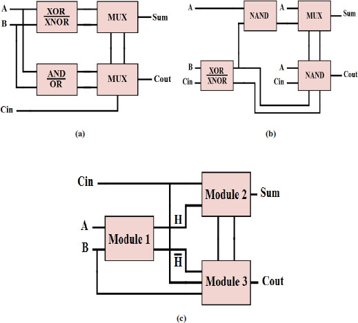
Figure 1. Different structures for implementing a full adder circuit: (a) Aguirre’s model (b) Kumar’s model (c) Hybrid model
Table 1. Logic equations for 1-bit full adder
Structure |
Sum |
Cout |
In the proposed work, a 1-bit energy efficient hybrid full adder is designed. The circuit utilizes 14 MOS transistors. The proposed full adder circuit shows lesser power dissipation and lesser power-delay product as compared to some of the previous related works. The effect of temperature on power dissipation has also been assessed in the proposed adder circuit by varying the temperature.
Therefore, a low power application has been identified as a prime concern for a Very Large Scale Integration (VLSI) system, which consumes less power and provides better battery life [Wairya et al. 2011]–[Goel et al. 2006]. Full adder is the fundamental building block in a portable device, which can be addressed through different logic designs to improve the battery life and decrease the silicon area i.e., by reducing the number of transistors [Goel et al. 2006]–[Hassoune et al. 2010]. Nevertheless, different logic designs (i.e., static and dynamic approach), performance metrics (i.e., power dissipation and delay) and number of transistors used in the designs are some of the fundamental parameters that have been studied by the researcher at different voltage ranges and technology scale (nano-technology) [Bhattacharyya et al. 2015], [Tirumalasetty et al. 2019], [Abid et al. 2008].
On the basis of the study, mainly different logic styles are used to design the full adder such as; static and dynamic CMOS [Bhattacharyya et al. 2015], [Goel et al. 2006], [Amini-Valashan et al. 2018], [Sun et al. 2014], ratioed style [Wairya et al. 2012], complementary pass-transistor logic (CPL) [Bhattacharyya et al. 2015], [Hasan et al. 2019], [Aguirre-Hernandez et al. 2011], [Nadu et al. 2014], Transmisión Gate (TG)-CMOS [Goel et al. 2003], [Janwadkar et al. 2018], [Hassoune et al. 2010], [Aguirre-Hernandez et al. 2011], Static Energy Recovery Full (SERF) [ Wairya et al. 2011], [Goel et al. 2006], [Venkatesan et al. 2019], [Yadav et al. 2018], carbon nanotube Field Effect Transistor (FET) [Dokania et al. 2018], Gate Diffusion Input (GDI) [Hasan et al. 2019], [Venkatesan et al. 2019], [Badry et al. 2018] and their hybrid arrangement [Wairya et al. 2011], [Bhattacharyya et al. 2015], [Kandpal et al. 2019], [Hasan et al. 2019], [Tirumalasetty et al. 2019], [Naseri et al. 2018], [Aguirre-Hernandez et al. 2011], [Nadu et al. 2014], [Yadav et al. 2018], [Dwivedi et al. 2016].
Every design has got their merits and demerits, for example, a static full adder is more reliable than dynamic full adder and consumes less power, whereas the dynamic full adder has faster switching speed in comparison to static full adder. Also, for N input logic, dynamic adder requires only (N+2) number of transistors whereas the static one requires 2N transistors. On the other hand, the voltage swing restoration of CPL is better in comparison to CMOS which contributes to low power consumption due to low voltage swing at the internal node. However, it suffers from static power consumption [Bhattacharyya et al. 2015], [Goel et al. 2006], [Hassoune et al. 2010], [Aguirre-Hernandez et al. 2011], whereas, voltage scaling [Dokania et al. 2018] of CMOS is better in comparison to CPL [Wairya et al. 2012], [Bhattacharyya et al. 2015], [Naseri et al. 2018]. Thus, the different logic styles have their own advantages and disadvantages, which is mainly dependent on power consumption, chip area and reliability constraint [Dokania et al. 2018], [Bhattacharyya et al. 2015], [Kandpal et al. 2019], [Naseri et al. 2018], [Amini-Valashan et al. 2018], [Abid et al. 2008], [Dwivedi et al. 2016]. Hence, finding the optimum solution to designing a full adder is considered an open research challenge for the researcher.
The notable work reported for 1-bit hybrid full adder circuit using GDI and CMOS technique at 120 nm technology simulated using Microwind VLSI CAD tool was described in [Nadu et al. 2014]. It was shown that, at supply voltage of 1.2 V, the proposed circuit provides better performance in terms of power dissipation and delay of 9 μW and 18 ps when compared with the conventional CMOS. Further, the silicon area size can be reduced due to the lesser transistor count (21T) when compared with the number of transistors (28T) in conventional CMOS [Nadu et al. 2014].
P. Bhattacharyya et al., reported the work based on hybrid arrangement of CMOS logic and TGL (transmission gate logic) using 16 transistors (16T) for low power and high speed application [Bhattacharyya et al. 2015]. It was shown in [Bhattacharyya et al. 2015], the hybrid circuit has better delay response when compared with the other existing models. The simulation was carried out for both 180 nm and 90 nm technology. The best performance in terms of power dissipation and delay was found to be 112.79 μW and 5.57 ns at 1.8V supply voltage for 180 nm technology and 53.36 μW and 2.45 ns at 1.2V supply voltage respectively. This was achieved due to the efficient pairing of strong transmission gates with the CMOS inverters [Bhattacharyya et al. 2015].
On the other hand, A. K. Yadav et al., presented 1-bit FA for low power application using 10T configuration designed at 45 nm CMOS technology using the HSIPCE software [Yadav et al. 2018]. It was reported that, the circuit presented in [Yadav et al. 2018], provides the maximum amount of improvement in PDP of 96.01% and 91.64% for GDI and SERF respectively. The hybrid combination of 1-bit adder using CPL, CMOS, and TG logic using 13T configuration for 90 nm technology is reported in [Kadu et al. 2018]. It was shown that considerable decrease in delay can be obtained by decreasing the transistor count i.e., delay of 5.18 ns and 20.03 ns is obtained using 13T and 16T full adder configuration.
Naseri and Timarchi presented the study of different type of logic for the implemented XOR/ XNOR gates for 65-nm technology using CMOS [Naseri et al. 2018]. Simulation were carried out using HSPICE and Cadence software and showed that the best results were obtained using hybrid FA-22T cell configuration, saving 43.5% energy delay product (EDP) and 23. 4% PDP when simulated over 0.65 to 1.5 V voltage range. Further, the study also presented the device sizing, which was obtained with the help of particle swarm optimization (PSO) algorithm [Naseri et al. 2018].
From the above discussion, it can be inferred that the 1-bit adder circuits design using the hybrid combination can provide an overall improvement in system performance. As different logic has different merits and demerits, therefore, in this we propose the new novel hybrid 1-bit adder using 14 T configurations, simulated at 130 nm technology using Mentor Graphics tool at 27 °C. The primary aim of this research work is to design the full adder circuit, which can provide the optimum solution in term of propagation delay and power dissipation. In Section 2 the schematic of the proposed hybrid 1-bit FA circuit and its operation is presented, as well as its comparison with other existing full adder. Section 3 deals with the results and analysis of the proposed 1-bit hybrid full adder and finally the conclusion is presented in Section 4.
2. Design and Simulation Setup of the Proposed 1-Bit Hybrid Full Adder
The schematic of the proposed 1-bit hybrid full adder circuit is shown in Figure 1, which is designed using fourteen (14) transistors. As observed from Figure 1, the hybrid arrangement of the proposed 1-bit hybrid full adder consists of three modules i.e., Module 1, Module 2 and Module 3 respectively (shown with color box). As shown in Figure 2, Module 1 arrangement has circuit of XOR-XNOR [Dokania et al. 2018], [Goel et al. 2006]–[Janwadkar et al. 2018], [Naseri et al. 2018], designed using six transistors based on the inverter configuration i.e., Tn1, Tp1, Tn2, Tp2, Tn3, Tp3 respectively. The advantage of using the XOR-XNOR circuit is that it reduces the complexity of the circuit as only half the number of transistor is required as compared with the conventional CMOS XOR circuit [ Wairya et al. 2011], [Tung et al. 2007], [Amini-Valashan et al. 2018]. Thus, it results in reducing the number of internal node, which further provides the reduction in power dissipation.
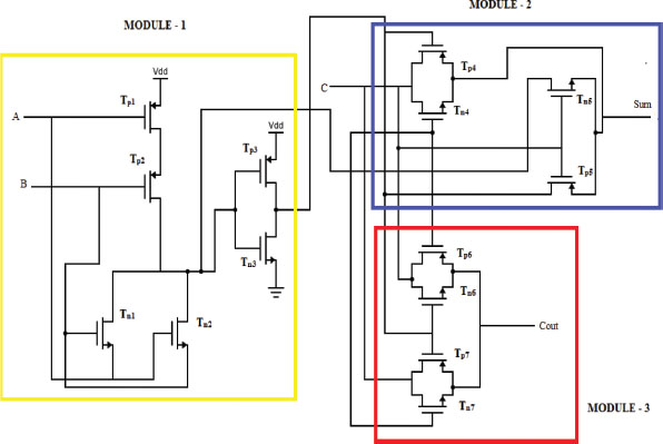
Figure 2. Design structure of the proposed 1-bit hybrid full adder for low power application (Different colors are used to distinguish between different modules).
The output generated from Module 1 (using two inputs A and B) is coupled with Module 2 and Module 3. Input C is connected to Module 2 and Module 3 respectively. Module 2 consists of a pair of transistors (Tn4, Tp4, Tn5, Tp5) responsible for sum (SUM) output signal, whereas Module 3 consists of transmission gate logic (Tn6, Tp6, Tn7, Tp7 ) responsible for carry output (Cout) signal. Carry propagation delay is reduced by TGL which further provides reduction in the overall propagation delay.
As discussed earlier, module-1 is a XOR-XNOR circuit which further drives module-2 and module-3. Elaborated discussions on all these modules are presented below:
Module-1 in Figure 2 is XOR-XNOR logic cell which generates output signals and acts as a driving input source to successive modules. Module 1 is responsible for maximum power dissipation. Since module 1, which consists of six transistors (6T), will provide full swing, so for swing restoration no extra transistors are required. Due to no direct path between power supply and ground, short- circuit current has been reduced which provides good driving capability, thus providing the robustness to the circuit. The major advantage of this module is that for all input combinations, both outputs have perfect voltage level.
Module-2 of the proposed full adder is PTL and Transmission gate based XOR gate. The function of this module is to implement SUM output. The outputs of module-1 serve as the inputs for module-2 while another input signal, (Cin) is provided externally. There are in total 4 transistors required for implementing the SUM output. Both XOR and its compliment are generated from module-1. Therefore, additional transistors are not required for to design the inverter that would complement the input XOR in module-2. The major advantage of this module is that it provides full swing output for all inputs and has lesser transistor count thus, resulting in low power dissipation.
Module-3 is based on TG logic and is built by connecting nMOS and pMOS transistors in parallel and controlled by the complementary control signals. When turned on simultaneously, both transistors (nMOS and pMOS) provide the input logic “0” or “1” respectively. Hence no voltage drop problem whether the 0 or the 1 is passed through it.
Thus, the proposed one bit full adder is used for minimizing the power dissipation. Also, due to the lesser number of transistors (14 T configurations), the power dissipation at the internal node reduced which decreased the power dissipation. Also, the carry propagation delay was reduced due to the TG logic, which further improves the overall propagation delay.
The proposed 1-bit hybrid circuit of full adder designed on the Mentor graphic tool is shown in Figure 3 and the time domain waveform, obtained from proposed 1-bit hybrid circuit of full adder at VDD =3V, is shown in Figure 4, this verifies the operation of the full adder circuits.
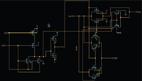
Figure 3. Simulated design of the proposed 1-bit hybrid full adder on Mentor graphic tool at 130 nm technologies
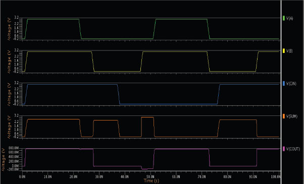
Figure 4. Time domain simulation waveform of the proposed 1 bit hybrid full adder at VDD =3V.
As a result, new complete adder architectures with low power dissipation and high speed are required. The 14T topology shown in Figure 2 is a full adder circuit. The adder chains integrated in the multiplier performed significantly better thanks to the compact circuit design and lower number of transistor counts. The low-power dissipation of adder topologies effectively minimizes the multiplier unit's overall power consumption and ensures energy-efficient low power computing.
Further, to make a comparison of performance, the proposed circuit of 1-bit hybrid full adder circuit was assessed along with the previous others 1-bit FA circuits reported in [ Wairya et al. 2012], [Dokania et al. 2018] (shown in Figure 5 (a) and Figure 5 (b) respectively) are simulated at 130 nm technology design using Mentor Graphics Tools at 100 MHz frequency.
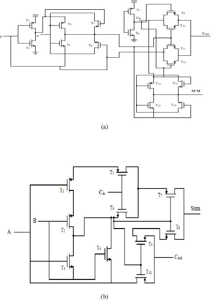
Figure 5. The schematic circuit design of 1-bit full adder (a) Using Hybrid 1-bit full adder, (b) Cell 3 full adder
The hybrid full adder (16T) circuit depicted in Figure 5(a) was created using transmission gates and a low power XOR-XNOR architecture. It has an internal node threshold voltage loss issue that has spread to the output nodes. Figure 5(b) shows Cell 3 Full Adder. The designs have unfavorable output voltage levels and poor operation. Therefore, it may be said that Cell 3 Full Adder and Hybrid Full Adder either have unsatisfactory output levels or unfavorable output voltage level. The design structure of the proposed full adder in Figure 2 exhibits full swing output level.
The performance of digital circuits and systems is measured through parameters such as power dissipation, delay and power delay product. The power dissipated in digital circuits is classified into two categories: Static and dynamic power. The total power dissipated in any digital circuit is called average power dissipation (Pavg). Static power dissipation occurs due to leakage current in the circuit when it is in idle or standby mode. Theoretically, in standby mode a CMOS digital circuit does not dissipate power because either pull-up network or pull-down network is in OFF state, which prevents leakage current. In a practical situation, a certain amount of power passes through the transistors. Static power dissipation associated with each transistor due to leakage current is quite small; however, when millions of transistors are integrated together, their cumulative effects become significant. The other type of power dissipation is dynamic power, which occurs while the device is in active state and is further classified into short-circuit power and switching power dissipation. The power dissipated in the charging and discharging of load capacitances is termed as switching power. The portion of power dissipation due to the flow of current from supply voltage (Vdd) directly to the ground terminal is called short-circuit power.
To evaluate the performance, the comparison is carried out using three metric viz. power dissipation, propagation delay and PDP. Propagation delay (TPropagation) depends on the chip area of the transistors (due to the scaling of transistors) and power dissipation and power delay product (PDP) in the circuit is given as:
where Ileakage, Vdd, f, CL, ISC represents leakage current, supply voltage, switching frequency, output capacitance, short circuit current:
The propagation delay is the time needed for an input signal to reach to the output. It can be calculated by taking the time difference of the 50% transition points of the output and input waveforms.
The Power Delay Product (PDP) in any logic circuit is defined as the product of the power dissipation of the circuit and the propagation delay. Reduction in power dissipation and delay greatly improves the efficiency of digital circuits. An energy efficient digital circuit has lesser PDP.
3. Results and Discussion
The comparative performance parameters using the proposed 1-bit hybrid full adder, along with the existing other 1-bit full adder presented in [Wairya et al. 2012], [Dokania et al. 2018] for the voltage range of 1 V to 3 V (volts) at 130-nm technology using Mentor Graphics is shown in Table 2.
Table 2. Performance Parameters Comparison of Full Adder (1.0 V to 3.0 V)
Vdd (V) |
1.0 |
1.8 |
2.0 |
3.0 |
Power Dissipation (nW) |
||||
Hybrid FA |
12.80 |
27.60 |
52.58 |
84.10 |
Cell 3 FA |
10.20 |
22.08 |
39.38 |
62.30 |
Proposed FA |
1.10 |
7.18 |
9.20 |
33.12 |
Delay (nS) |
||||
Hybrid FA |
19.80 |
19.90 |
17.48 |
16.10 |
Cell 3 FA |
28.20 |
26.17 |
24.32 |
19.95 |
Proposed FA |
15.90 |
15.20 |
12.80 |
9.10 |
Power Delay Product ( x 10-18J) |
||||
Hybrid FA |
253.44 |
594.24 |
919.09 |
1354.01 |
Cell 3 FA |
287.64 |
577.83 |
957.72 |
1242.88 |
Proposed FA |
17.49 |
109.136 |
117.76 |
301.39 |
As shown in Figure 6 (a), the hybrid FA circuit presented in [Wairya et al. 2012] does not show any improvement in power consumption (shown in nW) when compared with Cell 3 FA [Dokania et al. 2018], whereas the proposed hybrid circuit outperforms both of the existing 1-bit full adder circuits. The average improvement in power dissipation of 31.62 nW and 20.84 nW is obtained using proposed 1-bit hybrid full adder when compared with the Hybrid FA [Wairya et al. 2012] and Cell 3 FA [Dokania et al. 2018] respectively. Similarly, the simulated results obtained in Figure 6(b), for delay (shown in ns) shows, that the cell 3 FA shows poor performance when compared with existing hybrid FA [Wairya et al. 2012]. However, our proposed 1-bit hybrid full adder shows better performance when compared with previously existing full adder. It provides an average improvement in propagation delay of 5.07 ns and 11.41 ns when compared with the Hybrid FA [ Wairya et al. 2012] and Cell 3 FA [Dokania et al. 2018] respectively. It can be inferred from Figure 6(c), that the total PDP of both (previous existing adder) 1-bit full adder was almost similar, due to the fact that, one provides better power consumption while failing to provide any improvement in the propagation delay and vice versa.
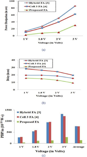
Figure 6. Comparative performance of the simulation results using proposed 1-bit hybrid adder circuit when compared with existing 1-bit adder in terms of, (a) Power dissipation (in nW), (b) Delay (in nS), (c) Power delay product (PDP in 10-18 W-s)
Thus, our proposed 1-bit hybrid full adder shows improvement in both power dissipation and propagation delay, therefore, improving the PDP of the proposed circuit as shown in Figure 6(c).
3.1. Temperature Analysis
In today’s era, where a large number of integrated circuits are fabricated on small area size die; a small temperature variation can significantly affect the overall performance. With the rise in temperature, the leakage current in any logic circuit also increases. To analyze the effect of temperature on the power dissipation of the proposed circuit, temperature ranges from -300C to 700C have been simulated. The power dissipation increases almost linearly with increase in temperature at lower temperature ranges and increases exponentially with further increase in temperature. Figure 7 shows the temperature variation effect on the power dissipation of the proposed adder circuit. The power dissipation increases at higher temperature ranges due to the increase in leakage current.
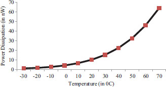
Figure 7. The effect of temperature variation on the power dissipation of the proposed circuit
4. Conclusion
The main objective of this research work was to design an efficient, low power, high speed adder circuit that can be integrated on a chip, making it a suitable and efficient choice for IOT applications. Energy efficient, low power 1-bit hybrid adder circuit is proposed in this paper, which provides better power dissipation and reduction in propagation delay, making it ideally suitable for low power application. The proposed 1-bit hybrid full adder provides the average power dissipation of 12.65 nW and average delay of 13.25 ns for voltage range between 1V to 3V volt. As the proposed circuit is designed using 14 T configuration, the area on the chip is also reduced. The proposed hybrid full adder circuit can be used in other different circuits such as multiplier, compressor and biomedical devices. It can detect faults in real time and can be used to design low power digital processing systems.
5. References
Chen S. L., C. H. Liao, T. K. Chi, T. L. Lin, And C. A. Chen, 2018 “Flexible Signals and Images Lossless Compression Chip Design for IoT and Industry 4.0,” in Proceedings of 14th IEEE/ASME International Conference on Mechatronic and Embedded Systems and Applications, pp. 1–6. DOI: https://doi.org/10.1109/MESA.2018.8449205
Giordani, M., M. Polese, M. Mezzavilla, S. Rangan, And M. Zorzi, 2019 “Towards 6G Networks: Use Cases and Technologies,” IEEE Communications Magazine, vol. 58, no. 3, pp. 55–61, Mar. DOI: https://doi.org/10.1109/MCOM.001.1900411
Wairya, S., R. K. Nagaria, And S. Tiwari, 2012 “Comparative Performance Analysis of XOR- XNOR Function Based High-Speed CMOS Full Adder Circuits For Low Voltage VLSI Design,” International Journal of VLSI design & Communication Systems (VLSICS), vol. 3, no. 2, pp. 432–436, DOI: https://doi.org/10.5121/vlsic.2012.3219
Dokania, V., R. Verma, M. Guduri, And A. Islam, 2018. “Design of 10T full adder cell for ultralow-power applications,” Ain Shams Engineering Journal, vol. 9, no. 4, pp. 2363–2372, DOI: https://doi.org/10.1016/j.asej.2017.05.004
Wairya, S., G. Singh, Vishant, R. K. Nagaria, And S. Tiwari, 2011 “Design analysis of XOR (4T) based low voltage CMOS full adder circuit,” in Proceedings of Nirma University International Conference on Engineering, pp. 1–7. DOI: https://doi.org/10.1109/NUiConE.2011.6153275.
Bhattacharyya, P., B. Kundu, S. Ghosh, V. Kumar, And A. Dandapat, 2015. “Performance Analysis of a Low-Power High-Speed Hybrid 1-bit Full Adder Circuit,” IEEE Transactions on Very Large Scale Integration (VLSI) Systems, vol. 23, no. 10, pp. 2001–2008, DOI: https://doi.org/10.1109/TVLSI.2014.2357057
Goel, S., A. Kumar, And M. A. Bayoumi, 2006. “Design of robust, energy-efficient full adders for deep-submicrometer design using hybrid-CMOS logic style,” IEEE Transactions on Very Large Scale Integration (VLSI) Systems, vol. 14, no. 12, pp. 1309–1321, DOI: https://doi.org/10.1109/TVLSI.2006.887807
Goel, S., M. A. Elgamel, And M. A. Bayoumi, 2003 “Novel design methodology for high-performance XOR-XNOR circuit design,” in Proceedings of 16th Symposium on Integrated Circuits and Systems Design, pp. 71–76. DOI: https://doi.org/10.1109/SBCCI.2003.1232809
Janwadkar, S. And S. Das, 2018, “Design and Performance Evaluation of Hybrid Full Adder for Extensive PDP Reduction,” in Proceedings of 3rd International Conference for Convergence in Technology, pp. 1–6. DOI: https://doi.org/10.1109/I2CT.2018.8529780
Kandpal, J., A. Tomar, S. Adhikari, and V. Joshi, 2019, “Design of Low Power and High Speed XOR/XNOR Circuit using 90 nm CMOS Technology,” in Proceedings of 2nd International Conference on Innovations in Electronics, Signal Processing and Communication, pp. 221–225. DOI: https://doi.org/10.1109/IESPC.2019.8902392
Hasan, M., U. K. Saha, A. Sorwar, M. A. Z. Dipto, M. S. Hossain, And H. U. Zaman, 2019, “A Novel Hybrid Full Adder Based on Gate Diffusion Input Technique, Transmission Gate and Static CMOS Logic,” in Proceedings of 10th International Conference on Computing, Communication and Networking Technologies, pp. 1–6. DOI: https://doi.org/10.1109/ICCCNT45670.2019.8944888
Hassoune, I., D. Flandre, I. O’connor, And J. D. Legat, 2010. “ULPFA: A new efficient design of a power-aware full adder,” IEEE Transactions on Circuits and Systems I: Regular Papers, vol. 57, no. 8, pp. 2066–2074, DOI: https://doi.org/10.1109/TCSI.2008.2001367
Tirumalasetty, V. R., And M. R. Machupalli, “Design and analysis of low power high-speed 1-bit full adder cells for VLSI applications,” International Journal of Electronics, vol. 106, no. 4, pp. 521–536, 2019. DOI: https://doi.org/10.1080/00207217.2018.1545256
Naseri, H., And S. Timarchi, 2018. “Low-Power and Fast Full Adder by Exploring New XOR and XNOR Gates,” IEEE Transactions on Very Large Scale Integration (VLSI) Systems, vol. 26, no. 8, pp. 1481–1493, DOI: https://doi.org/10.1109/TVLSI.2018.2820999
Tung, C. K., Y. C. Hung, S. H. Shieh, And G. S. Huang, 2007, “A low-power high-speed hybrid CMOS full adder for embedded system,” in Proceedings of the 2007 IEEE Workshop on Design and Diagnostics of Electronic Circuits and Systems, DDECS, pp. 199–202. DOI: https://doi.org/10.1109/DDECS.2007.4295280
Amini-Valashani, M., M. Ayat, And S. Mirzakuchaki, 2017, “Design and analysis of a novel low-power and energy-efficient 18T hybrid full adder,” Microelectronics Journal, vol. 74, pp. 49–59, 2018. DOI: https://doi.org/10.1016/j.mejo.2018.01.018
Abid, Z., H. El-Razouk, And D. A. El-Dib, 2008. “Low power multipliers based on new hybrid full adders,” Microelectronics Journal, vol. 39, no. 12, pp. 1509–1515, DOI: https://doi.org/10.1016/j.mejo.2008.04.002
Sun, Y., And V. Kursun, 2014. “Carbon nanotubes blowing new life into NP dynamic CMOS circuits,” IEEE Transactions on Circuits and Systems I: Regular Papers, vol. 61, no. 2, pp. 420–428, DOI: https://doi.org/10.1109/TCSI.2013.2268131
Aguirre-Hernandez, M. And M. Linares-Aranda, 2011 “CMOS Full-Adders for Energy-Efficient Arithmetic Applications,” IEEE Transactions on Very Large Scale Integration (VLSI) Systems, vol. 19, no. 4, pp. 718–721. DOI: https://doi.org/10.1109/TVLSI.2009.2038166
Nadu, T., S. Mohan, and N. Rangaswamy, 2014, “Performance Analysis of 1 bit Full Adder Using GDI Logic,” in Proceedings of International Conference on Information Communication and Embedded Systems (ICICES2014), no. 978, pp. 1–4. DOI: https://doi.org/10.1109/ICICES.2014.7034029
Venkatesan, C., M. Thabsera Sulthana, M. G. Sumithra, And M. Suriya, 2019, “Analysis of 1- bit full adder using different techniques in Cadence 45nm Technology,” in Proceedings of 5th International Conference on Advanced Computing and Communication Systems, pp. 179–184. DOI: https://doi.org/10.1109/ICACCS.2019.8728449
Yadav, A. K., B. P. Shrivatava, And A. K. Dadoriya, 2018, “Low power high speed 1-bit full adder circuit design at 45nm CMOS technology,” in Proceedings of International Conference on Recent Innovations in Signal Processing and Embedded Systems, pp. 427–432. DOI: https://doi.org/10.1109/RISE.2017.8378203
Badry, O. Al And M. A. Abdelghany, 2018, “Low power 1-Bit full adder using Full-Swing gate diffusion input technique,” in Proceedings of 2018 International Conference on Innovative Trends in Computer Engineering, vol. 2018-March, no. ITCE, pp. 205–208. DOI: https://doi.org/10.1109/ITCE.2018.8316625
Dwivedi, S., K. Khare, And A. K. Dadoria, 2016, “Low-Power High Speed 1-bit Full Adder Circuit Design,” in Proceedings of the Second International Conference on Information and Communication Technology for Competitive Strategies, pp. 1–5. DOI: https://doi.org/10.1145/2905055.2905321
Kadu C. P., And M. Sharma, 2018, “Area-Improved High-Speed Hybrid 1-bit Full Adder Circuit Using 3T-XNOR Gate,” in Proceedings of International Conference on Computing, Communication, Control and Automation, pp. 1–5. DOI: https://doi.org/10.1109/ICCUBEA.2017.8463827.
Notes of Contributors
Rahul Mani Upadhyay received the B.Tech. degree in Electronics and Communication Engineering, the M. Tech. degree in Electronic Design and Technology from Uttar Pradesh Technical University, Lucknow, India in 2010 and 2013 respectively and currently pursuing Ph.D. degree in VLSI and Microelectronics from Madan Mohan Malaviya University of Technology, Gorakhpur, India. His current research interests include digital systems, VLSI design, and low-power and ultra low power digital ircuits.
Dr. Rajeev Kumar Chauhan received the Ph.D degree in Electronics Engineering from IIT-BHU, Varanasi in 2002 and ME from MNNIT – Allahabad in 1993 and B.Tech from G.B.P.U.A.T –Pantnagar in 1989. He has joined erstwhile Madan Mohan Malaviya Engineering College, Gorakhpur in 1993 as a Lecturer, as an Assistant Professor from 2002, as an Associate Professor from 2006 and Professor since 2017. The college has been reconstituted as Madan Mohan Malaviya University of Technology by U.P. State Government in 2013. He also worked as Professor in Department of ECE, Faculty of Technology, Addis Ababa University, Ethiopia between 2003 to 2005. He is author of more than 200 research papers published in Journals and Conferences. His current research interests include emerging nanoscale devices and issues in in VLSI as well as circuits and systems.
Dr. Manish Kumar received Ph.D. degree in VLSI and Microelectronics from IIT (ISM) Dhanbad, India in 2014. He is Associate Professor in the Department of Electronics and Communication Engineering, Madan Mohan Malaviya University of Technology, Gorakhpur, India. His field of Specialization is VLSI design. He has received INSA-Visiting Fellowship by the Indian National Science Academy, New Delhi in the year 2012-13 and Selected as a UGC Dr. D.S. Kothari Post Doctoral Fellow (DSKPDF) in the year 2014-15. He is a member of Indian Science Congress Association, International Association of Engineers, Institution of Engineers (India), Indian Society for Technical Education, Semiconductor Society of India and Institution of Electronics and Telecommunication Engineers.